5962-87591013X

Active - 12-BIT ADC (AD7572SE)
Description:
12-BIT ADC (AD7572SE)
5962-87591013X Specification
Product Attribute
Attribute Value
Sampling Rate (Per Second)
-
Number of A/D Converters
1
Voltage - Supply, Analog
-14.25V ~ -15.75V, 4.75V ~ 5.25V
Voltage - Supply, Digital
-14.25V ~ -15.75V, 4.75V ~ 5.25V
Operating Temperature
-55 ℃ ~ 125 ℃
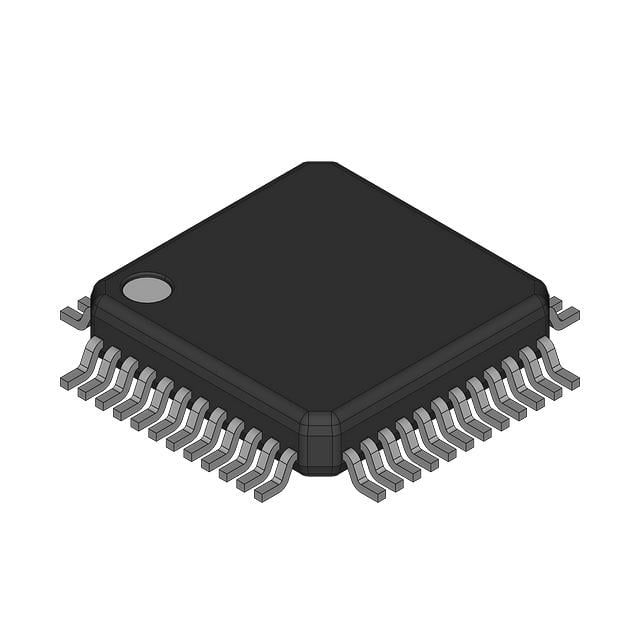
Supplier Device Package
28-CLCC (11.43x11.43)
Mounting Type
Surface Mount
5962-87591013X Description
Overview
The Analog Devices 5962-87591013X is a military-grade operational amplifier that belongs to the family of precision, high-speed, low-noise op-amps. It is compliant with MIL-STD-883 specifications and designed for use in demanding aerospace, defense, and high-reliability applications. This specific part number denotes a screened, high-reliability version of the ADOP07, which is well known for its ultra-low offset voltage and excellent long-term stability.
Package and Mounting
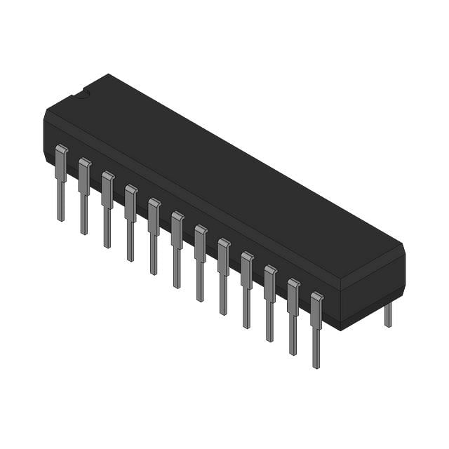
* Package Type: Metal can (TO-99-8)
* Package Style: Hermetically sealed for enhanced reliability
* Terminal Count: 8 leads
* Mounting Type: Through-Hole
Electrical Characteristics (Typical @ 25°C)
* Input Offset Voltage: 25 µV (max), 75 µV (max over temperature)
* Input Bias Current: 1.8 nA (typ), 4 nA (max)
* Input Offset Current: 0.2 nA (typ), 1.8 nA (max)
* Input Voltage Noise Density: 0.4 nV/√Hz @ 10 Hz
* Input Voltage Range: ±13 V minimum
* Common-Mode Rejection Ratio (CMRR): 114 dB (typ)
* Power Supply Rejection Ratio (PSRR): 120 dB (typ)
* Gain Bandwidth Product: 0.6 MHz
* Slew Rate: 0.3 V/µs
* Open-Loop Voltage Gain: 1,200,000 (min)
* Output Voltage Swing: ±10 V into 10kΩ load
Power Requirements
* Supply Voltage Range: ±3 V to ±18 V
* Supply Current: 1.2 mA (typ)
* Power Dissipation: Typically low, making it suitable for precision analog circuits
Temperature and Environmental Ratings
* Operating Temperature Range: −55°C to +125°C
* Storage Temperature Range: −65°C to +150°C
* MIL-STD-883 compliant screening
* Radiation tolerant (to some extent, depending on application-specific qualification)
Functional Features
* Extremely low input offset voltage drift: typically 0.3 µV/°C
* Long-term stability: 1.5 µV/month
* Low power consumption, ideal for precision and battery-operated systems
* Low bias and offset currents enable high input impedance configurations
* Excellent for instrumentation, medical, aerospace, and military-grade analog front ends
Applications
* Precision data acquisition systems
* Strain gauge and thermocouple amplifiers
* Low-level signal conditioning
* High-reliability aerospace and defense electronics
* Analog computation and control loops
* Medical instrumentation
Reliability and Screening
* This device is part of the JAN (Joint Army-Navy) program
* Screened according to MIL-PRF-38535
* Class B or S reliability options depending on the suffix
* Designed for extreme environments including radiation-prone and high-vibration systems
The Analog Devices 5962-87591013X represents a robust solution for engineers seeking extreme precision and long-term reliability in analog signal processing, especially under harsh environmental conditions.