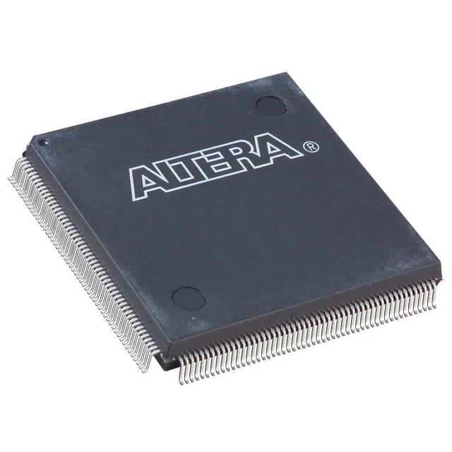
EP2C8T144C6

Active - IC FPGA 85 I/O 144TQFP
Description:
IC FPGA 85 I/O 144TQFP
EP2C8T144C6 Specification
Product Attribute
Attribute Value
Programmable
Not Verified
Number of Logic Elements/Cells
8256
Voltage - Supply
1.15V ~ 1.25V
Mounting Type
Surface Mount
Operating Temperature
0 ℃ ~ 85 ℃ (TJ)
Supplier Device Package
144-TQFP (20x20)
EP2C8T144C6 Description
The Intel EP2C8T144C6 is a member of the Cyclone II family of low-cost, low-power field-programmable gate arrays (FPGAs) designed for cost-sensitive applications requiring moderate logic density, flexible I/O, and high integration. The device combines a reconfigurable logic array, embedded memory blocks, and programmable interconnects to support custom digital designs in applications such as digital signal processing, communication systems, industrial control, and consumer electronics. The EP2C8T144C6 is fabricated using a 90 nm CMOS process, offering low static and dynamic power consumption, and is packaged in a 144-pin Thin Quad Flat Pack (TQFP), providing a compact solution for board-level integration.
## Logic Array and Capacity
The EP2C8T144C6 features 8,256 logic elements (LEs), which are the basic building blocks for implementing combinational and sequential logic functions. Each logic element includes a 4-input look-up table (LUT) and a flip-flop, allowing the implementation of a wide variety of logic functions. The device supports a variety of user-configurable logic structures, including small arithmetic functions, counters, multiplexers, and state machines. The Cyclone II architecture optimizes area and speed for cost-sensitive applications while providing predictable performance across the logic array.
## Embedded Memory
The FPGA integrates 112 Kbits of embedded RAM, organized into 16 blocks of 4 Kbits each. This memory can be configured as single-port or dual-port RAM, FIFO buffers, or shift registers, supporting data storage and high-speed buffering within the logic fabric. The embedded memory operates synchronously with the FPGA’s internal clock and supports byte-wide access, enabling efficient implementation of data-intensive applications such as packet buffering, signal processing, or temporary storage for arithmetic operations.
## I/O Architecture
The EP2C8T144C6 provides 98 user I/O pins in the TQFP-144 package, with configurable voltage standards including 1.5 V, 1.8 V, 2.5 V, 3.3 V LVTTL, and LVCMOS. The I/O blocks support programmable slew rate control and optional on-chip termination, providing flexibility for interfacing with a variety of external devices and high-speed signaling standards. I/O pins can also be configured as dedicated global clock inputs, dedicated global set/reset signals, or as general-purpose bidirectional pins, providing versatile system-level integration.
## Clocking Resources
The device incorporates four global clock networks, enabling low-skew distribution of high-speed clock signals throughout the FPGA. These global networks support multiple clock domains and can drive large fan-outs with minimal delay. Dedicated clock input pins allow integration with external oscillators or PLLs to generate the required internal clock frequencies. The Cyclone II architecture also supports synchronous and asynchronous resets, as well as user-controlled phase relationships for complex timing schemes.
## PLLs and Frequency Management
The EP2C8T144C6 contains up to two phase-locked loops (PLLs) that allow frequency multiplication, division, and phase shifting of input clock signals. The PLLs support flexible clock management, enabling precise timing control and generation of multiple clock domains with different frequencies or phases. These PLLs are ideal for applications requiring high-speed serial interfaces, multi-rate digital signal processing, or clock-domain crossing with low jitter and minimal skew.
## Power Consumption
The Cyclone II family, including the EP2C8T144C6, is optimized for low static and dynamic power. Typical core voltage operation is 1.2 V, with I/O voltage levels configurable depending on application requirements. Core current consumption depends on logic utilization, clock frequency, and I/O toggling rates, with typical static current on the order of a few milliamperes at room temperature. Dynamic power scales linearly with operating frequency and toggling activity. The FPGA supports a partial power-down mode for unused logic to further reduce power consumption.
## Configuration and Programming
The EP2C8T144C6 is configured via a serial or parallel configuration interface, supporting both JTAG and active serial programming methods. Configuration data is stored in an external memory such as EEPROM or Flash and is loaded into the device on power-up. The FPGA also supports in-system reconfiguration, allowing dynamic reprogramming of logic while the system is operational. Configuration security features such as encryption and readback protection are available to protect intellectual property and prevent unauthorized access.
## Timing Characteristics
The Cyclone II FPGA provides moderate performance suitable for a wide range of cost-sensitive applications. Maximum internal logic speed is approximately 200 MHz under typical operating conditions. Combinational path delays are minimized through dedicated routing resources, while flip-flop setup and hold times are optimized for predictable timing closure. Input-to-output propagation delays depend on logic depth and routing but remain suitable for medium-speed digital processing. Timing analysis is supported through Intel Quartus Prime software, enabling designers to verify performance and optimize critical paths.
## Reliability and Environmental Specifications
The EP2C8T144C6 operates over a commercial temperature range of 0°C to 85°C, with storage and soldering temperatures conforming to standard TQFP handling specifications. The device is designed for long-term reliability, with CMOS-level junction robustness, ESD protection on all I/O pins, and adherence to lead-free RoHS compliance. Thermal dissipation depends on logic activity, package type, and PCB layout, with recommended thermal management for sustained high-frequency operation.
## Applications
The EP2C8T144C6 is suitable for a wide variety of applications:
* Consumer electronics and multimedia devices
* Industrial automation and control systems
* Communication interfaces and protocol bridging
* Digital signal processing and data acquisition
* Low-cost prototyping and development platforms
* Embedded systems requiring flexible, reconfigurable logic
## Key Specifications
* Logic Elements: 8,256
* Embedded Memory: 112 Kbits
* User I/O Pins: 98
* Global Clock Networks: 4
* PLLs: 2
* Core Voltage: 1.2 V typical
* I/O Voltage Standards: 1.5 V, 1.8 V, 2.5 V, 3.3 V
* Maximum Operating Frequency: 200 MHz typical
* Package: 144-pin TQFP
* Operating Temperature: 0°C to 85°C
* Power Dissipation: depends on logic utilization and clock frequency
## Performance Considerations
Designers should consider the balance between logic utilization, I/O toggling rate, and clock frequency to manage dynamic power and thermal performance. Critical timing paths should be verified using timing analysis tools, and proper decoupling is recommended to minimize noise and maintain signal integrity. PLLs should be configured to provide stable, low-jitter clock signals for high-speed interfaces. PCB layout must consider power and ground planes, trace impedance, and thermal paths to ensure optimal performance and reliability.
## Summary
The Intel EP2C8T144C6 Cyclone II FPGA provides a flexible, cost-effective solution for medium-density, moderate-speed digital applications. With 8,256 logic elements, embedded memory, configurable I/O, PLLs, and low-power operation, it supports a wide range of signal processing, control, and interface applications while maintaining predictable performance, reliability, and ease of integration.


 Spain