ICL7667CBA

Obsolete - DUAL POWER MOSFET DRIVER
Description:
DUAL POWER MOSFET DRIVER
ICL7667CBA Specification
Product Attribute
Attribute Value
Gate Type
N-Channel MOSFET
Voltage - Supply
4.5V ~ 17V
Logic Voltage - VIL, VIH
0.8V, 2V
Current - Peak Output (Source, Sink)
-
High Side Voltage - Max (Bootstrap)
-
Rise / Fall Time (Typ)
20ns, 20ns
Operating Temperature
0 ℃ ~ 150 ℃ (TJ)
Mounting Type
Surface Mount
Package / Case
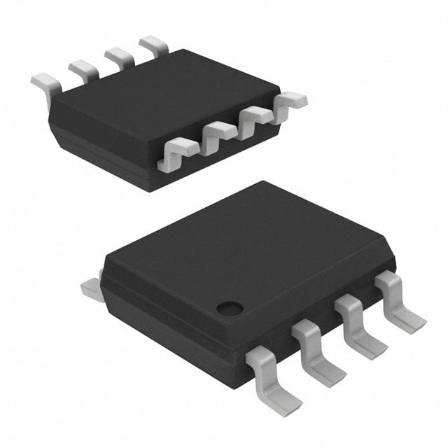
8-SOIC (0.154", 3.90mm Width)
Supplier Device Package
8-SOIC
ICL7667CBA Description
Product Overview
The Renesas Electronics ICL7667CBA is a dual high-speed MOSFET driver designed to drive both n-channel and p-channel power MOSFETs in high-speed switching applications. Originally developed by Intersil and now under Renesas, this IC is optimized for switching power supplies, DC-DC converters, pulse generators, and motor drive circuits. With both sourcing and sinking capability and very fast transition times, it provides robust gate control in demanding applications.
Function and Architecture
The ICL7667CBA integrates two independent non-inverting MOSFET drivers into a single package. Each driver is capable of sourcing and sinking large peak currents into capacitive loads, such as the gate of a power MOSFET. These drivers eliminate the need for discrete push-pull buffer stages, simplifying designs and improving performance.
* Driver Channels: 2 (independent, non-inverting)
* Input Type: TTL/CMOS compatible logic-level inputs
* Output Type: High-speed push-pull driver
* Output Drive Configuration: Totem-pole (active sourcing and sinking)
Electrical Characteristics
The ICL7667CBA is capable of delivering high peak currents with minimal delay, allowing it to rapidly charge and discharge MOSFET gates. This ensures efficient switching with reduced transition losses and minimized shoot-through currents in half-bridge or full-bridge configurations.
* Supply Voltage (V+): 4.5 V to 18 V
* Output Voltage Swing: Rail-to-rail (close to GND and V+)
* Peak Output Current (per channel): ±1.5 A typical
* Continuous Output Current: 200 mA typical
* Low-Level Output Voltage (VOL): <0.4 V at IOUT = 20 mA
* High-Level Output Voltage (VOH): > V+ – 0.25 V at IOUT = –20 mA
* Input Threshold Voltage:
– VIL: ≤0.8 V
– VIH: ≥2.0 V
* Input Current: ±1 µA max
Switching Performance
The ICL7667CBA is designed for high-speed operation, enabling fast switching of power devices and supporting high-frequency converter designs. Fast rise and fall times allow for efficient gate drive even at elevated frequencies.
* Rise Time (tr): 20 ns typical with 1000 pF load
* Fall Time (tf): 20 ns typical with 1000 pF load
* Propagation Delay Time: 35 ns typical
* Switching Frequency: >1 MHz operation possible depending on load
Power and Thermal Ratings
The device is capable of operating over a wide supply voltage and temperature range, with adequate thermal handling capabilities for moderate power applications. For higher thermal demands, PCB layout and cooling enhancements are recommended.
* Power Dissipation:
– ~470 mW typical at TA = 25°C (depends on load and switching frequency)
* Junction-to-Ambient Thermal Resistance (θJA): ~130°C/W (standard PCB)
* Operating Temperature Range (TA): 0°C to +70°C
* Storage Temperature: –65°C to +150°C
Applications
The ICL7667CBA is intended for driving the gates of power MOSFETs or IGBTs in applications that demand rapid and efficient gate charging and discharging.
* Switching power supplies
* DC-DC converters (synchronous and asynchronous)
* Class D audio amplifiers
* Motor control drivers
* High-speed pulse generators
* Logic-level to power-level translation
Package and Pin Configuration
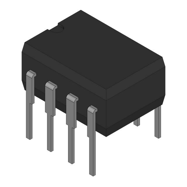
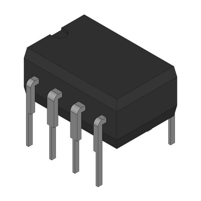
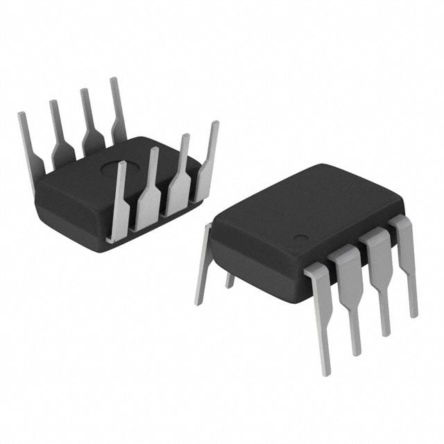
The ICL7667CBA is supplied in a standard 8-lead plastic DIP package (Dual In-line Package), making it suitable for both prototyping and through-hole production environments.
* Package Type: 8-lead PDIP
* Pin Count: 8
* Package Material: Epoxy mold compound
* Mounting: Through-hole
* Lead Pitch: 2.54 mm
* RoHS Compliant: Yes
Functional Pin Description
* IN A / IN B: Logic inputs for each driver (TTL/CMOS compatible)
* OUT A / OUT B: Gate drive outputs
* V+: Positive supply (shared for both channels)
* GND: Ground reference (shared)
Protection and Reliability Features
While the ICL7667CBA does not integrate advanced protection features like thermal shutdown or under-voltage lockout, its robust output stage and rail-to-rail operation allow for reliable performance in controlled environments. Input levels are protected against ESD and latch-up under normal operating conditions.
* Latch-Up Immunity: Improved CMOS structure with high latch-up resistance
* ESD Protection: Standard for CMOS devices (not specified for automotive-grade)
Summary of Key Specifications
* Channels: 2 non-inverting high-speed drivers
* Supply Voltage: 4.5 V to 18 V
* Peak Output Current: ±1.5 A
* Rise/Fall Time: 20 ns typical
* Propagation Delay: 35 ns typical
* Input Logic Compatibility: TTL/CMOS
* Output Drive: Rail-to-rail
* Operating Temp Range: 0°C to +70°C
* Package: 8-Pin DIP (PDIP)
The Renesas ICL7667CBA is a versatile, fast, and reliable dual MOSFET driver ideal for applications requiring efficient gate drive, low propagation delay, and compact through-hole packaging. It simplifies high-speed switching designs, especially in analog power control systems and high-efficiency power conversion stages.


 Lithuania