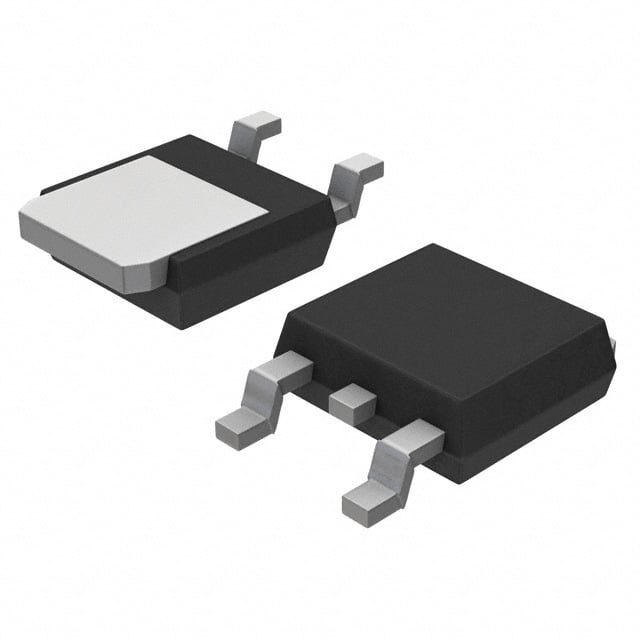
NCV317LBDR2G

Active - IC REG LIN POS ADJ 100MA 8SOIC
Description:
IC REG LIN POS ADJ 100MA 8SOIC
NCV317LBDR2G Specification
Product Attribute
Attribute Value
Series
Automotive, AEC-Q100
Packaging
Tape & Reel (TR)
Output Configuration
Positive
Voltage - Input (Max)
40V
Voltage - Output (Min/Fixed)
1.2V
Voltage - Output (Max)
37V
Current - Quiescent (Iq)
10 mA
Protection Features
Over Current, Over Temperature, Short Circuit
Operating Temperature
-40 ℃ ~ 125 ℃
Mounting Type
Surface Mount
Package / Case
8-SOIC (0.154", 3.90mm Width)
Supplier Device Package
8-SOIC
NCV317LBDR2G Description
Overview
The onsemi NCV317LBDR2G is a low dropout (LDO) linear voltage regulator designed to provide a fixed 5.0 V output with excellent precision and stability. It is tailored for automotive and industrial applications, featuring automotive-grade qualification with AEC-Q100 Grade 1 compliance, ensuring reliable operation in harsh environments. This regulator is optimized for systems requiring a stable, noise-free voltage source with low dropout voltage and robust protection features, supporting both analog and digital circuits in various electronic systems.
Key Features
The NCV317LBDR2G offers a fixed 5.0 V output voltage with a tight accuracy typically within ±2% over the full temperature range. It supports an input voltage up to 40 V, accommodating common automotive battery voltages and load dump conditions. The device exhibits a low dropout voltage, typically below 400 mV at full load current, which maximizes efficiency and allows operation from low-voltage supply rails.
Designed for automotive use, the NCV317LBDR2G incorporates extensive protection features including thermal shutdown, current limiting, and reverse battery protection. The device also has excellent transient response and low output noise, making it suitable for powering sensitive loads in automotive infotainment, engine control units (ECUs), and sensor systems.
Electrical Specifications
* Output Voltage: Fixed at 5.0 V with ±2% accuracy
* Input Voltage Range: 5.5 V to 40 V (supports load dump and cold crank conditions typical in automotive systems)
* Dropout Voltage: Typically 400 mV at 500 mA load current
* Maximum Output Current: Up to 500 mA continuous load
* Quiescent Current: Approximately 3 mA typical under no-load conditions
* Line Regulation: 0.01% per V typical
* Load Regulation: 0.3% typical from zero to full load
* Output Noise: Low noise suitable for sensitive applications
* Operating Temperature Range: -40°C to +125°C junction temperature compliant with automotive Grade 1
* Thermal Resistance: Junction-to-ambient approximately 70 °C/W in SOIC-8 package
Functional Description
The NCV317LBDR2G operates as a linear regulator utilizing an internal bandgap reference and error amplifier to maintain a constant 5.0 V output regardless of input voltage variations and load changes, within the device’s operating range. Its low dropout voltage design allows the regulator to maintain regulation even when the input voltage is near the output voltage, critical for maximizing battery life and efficiency.
The device includes an internal power transistor controlled by the error amplifier output, adjusting conduction to stabilize the output voltage. The regulator also supports reverse battery conditions, ensuring device protection during incorrect polarity connections in automotive environments.
Thermal shutdown circuitry monitors the junction temperature, disabling the output if excessive heat is detected, preventing damage from thermal stress. Current limiting protects the device and the powered circuitry from overload or short-circuit conditions by limiting output current to a safe maximum.
Protection Features
* Reverse Battery Protection: Device withstands negative input voltage connection without damage.
* Overcurrent Protection: Limits output current to prevent damage due to overload or short circuits.
* Thermal Shutdown: Automatically disables the device if junction temperature exceeds safe limits, resuming operation upon cooldown.
* Load Dump Protection: Supports transient input voltages up to 40 V, typical for automotive load dump scenarios.
* ESD Protection: Enhanced electrostatic discharge robustness suitable for automotive applications.
Typical Applications
* Automotive electronic control units (ECUs)
* Infotainment and navigation systems in vehicles
* Sensor and actuator power supplies in automotive and industrial systems
* Industrial automation and control systems
* Battery-powered and portable devices requiring stable 5 V power rails
* Communication equipment requiring robust voltage regulation
Package Information
The NCV317LBDR2G is offered in an SOIC-8 package with a thermal pad option, designed for surface-mount technology. The package measures approximately 5.0 mm x 4.9 mm, facilitating efficient PCB space usage and effective heat dissipation.
Absolute Maximum Ratings
* Input Voltage: -16 V (reverse polarity) to +45 V
* Output Voltage: -0.3 V to VIN + 0.3 V
* Storage Temperature: -65°C to +150°C
* Operating Junction Temperature: -40°C to +150°C
* Maximum Output Current: 500 mA (limited by thermal and current protection)
Typical Performance Parameters
* Dropout Voltage: 400 mV typical at 500 mA load
* Output Voltage Accuracy: ±2% across temperature and line/load conditions
* Quiescent Current: 3 mA typical
* Load Regulation: 0.3% from no load to full load
* Line Regulation: 0.01% per V
* Thermal Shutdown Threshold: Approximately 160°C
Pin Configuration
1. Input (VIN): Supply voltage input, supports wide automotive voltage range.
2. Ground (GND): Common ground reference.
3. Output (VOUT): Provides regulated 5.0 V output.
4-8. Other Pins: Typically connected internally or used for thermal and mechanical purposes depending on package variant.
Conclusion
The onsemi NCV317LBDR2G is a robust, automotive-qualified low dropout regulator delivering a stable 5.0 V output with high accuracy and wide input voltage tolerance. Its automotive-grade design, including reverse polarity and load dump protections, makes it especially suitable for demanding vehicular and industrial applications. The device’s low dropout voltage, combined with comprehensive protection features and low output noise, provides a reliable and efficient power source for sensitive analog and digital circuits. Its compact SOIC-8 package and excellent thermal performance further facilitate integration into space-constrained, high-reliability systems.
NCV317LBDR2G Stock: 20650
5.0 / 5.0

2021-08-12 12:06
IGBT transistors not detected SA for testerach beside plus t7-h, in tescie for przelaczanie with-12V for E plus zarowka powered + 12V for C triggered finger with Plus, zalancza with-wylancza. Very fast wysylka, fast delivery, product good jakosci, very we
2021-12-31 23:06
Good product and work correctly .
2021-07-09 02:45
Well received, not tested yet
2021-12-03 00:22
I order 10pcs. Now test three chips and two was ID 0x441, wich is STM32F412, not STM32F407. I am wery disapointed.
2021-12-27 06:22
The goods are very satisfied, the seller Thank you very much.