BUV20

Obsolete - TRANS NPN 125V 50A TO3
Description:
TRANS NPN 125V 50A TO3
BUV20 Specification
Product Attribute
Attribute Value
Current - Collector (Ic) (Max)
50 A
Voltage - Collector Emitter Breakdown (Max)
125 V
Vce Saturation (Max) @ Ib, Ic
1.2V @ 5A, 50A
Current - Collector Cutoff (Max)
3mA
DC Current Gain (hFE) (Min) @ Ic, Vce
20 @ 25A, 2V
Frequency - Transition
8MHz
Operating Temperature
200 ℃ (TJ)
Mounting Type
Chassis Mount
Package / Case
TO-204AA, TO-3
Supplier Device Package
TO-3
BUV20 Description
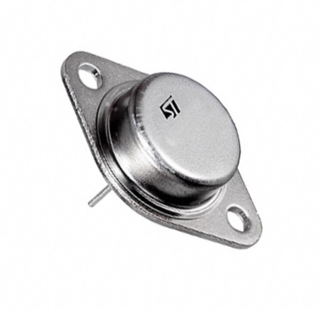
The STMicroelectronics BUV20 is a high-power NPN bipolar junction transistor (BJT) designed for switching and linear power amplification applications in medium- to high-voltage power electronics. It is part of STMicroelectronics’ high-voltage transistor portfolio optimized for industrial and energy conversion systems, where robust safe operating area (SOA), high collector current capability, and high power dissipation are required. The device is typically supplied in a TO-3 metal can package, which provides excellent thermal conductivity and mechanical robustness, making it suitable for high-power dissipation environments such as linear regulators, motor control stages, and power switching circuits.
## Device Function and Classification
The BUV20 is classified as a high-voltage NPN power transistor. Its primary function is to control large collector-emitter currents under the influence of a base drive current, enabling both switching and linear amplification operation modes. In switching applications, it operates as a saturated switch, while in linear operation it functions as a controllable current amplifier.
The device is designed for power stages where both voltage and current stresses are significant. Its silicon epitaxial planar structure is optimized to provide a wide safe operating area, ensuring stable performance under both DC and pulsed conditions. This makes it suitable for inductive load control, high-voltage switching, and linear regulation circuits where secondary breakdown robustness is critical.
## Electrical Characteristics
The BUV20 is specified with a collector-emitter voltage (V_CEO) typically rated at 400 V, allowing operation in high-voltage power circuits such as mains-derived supplies and industrial control systems. The collector current (I_C) is rated up to 15 A under defined thermal conditions, supporting substantial load drive capability.
The device exhibits a DC current gain (h_FE) specified over a range of collector currents, ensuring sufficient base drive efficiency for both switching and linear operation. Gain values decrease at higher collector currents, which is typical for high-power BJTs, and must be considered in driver stage design.
The collector-emitter saturation voltage (V_CE(sat)) is specified under forced beta conditions, representing conduction losses during saturated switching operation. Lower saturation voltage improves efficiency in switching applications by reducing power dissipation during conduction.
The transition frequency (f_T) defines the gain-bandwidth product of the device and indicates its suitability for moderate-speed switching applications. While not optimized for RF operation, it is adequate for power switching and control frequencies typical in industrial systems.
Power dissipation (P_tot) is a key parameter, typically in the range of hundreds of watts under ideal heatsinking conditions. This rating is strongly dependent on case temperature and thermal management design. Thermal resistance junction-to-case (R_thJC) is specified for the TO-3 package, enabling accurate thermal modeling for high-power operation.
The device also specifies a wide safe operating area (SOA), which defines permissible combinations of voltage and current under DC and pulsed conditions. This characteristic is critical in linear operation, where simultaneous high voltage and current stress can lead to secondary breakdown if exceeded.
## Functional Behavior and Operating Principles
The BUV20 operates based on bipolar junction transistor principles, where a small base current controls a much larger collector-emitter current. In switching mode, the device is driven into saturation, minimizing collector-emitter voltage drop and reducing conduction losses. In linear mode, it operates in the active region, allowing controlled amplification of input signals or regulation of output voltage/current.
Switching performance is governed by charge storage effects in the base region, which influence turn-on and turn-off times. Although not optimized for high-speed switching, the device is suitable for low- to medium-frequency power control applications. Proper base drive design is required to ensure fast saturation and avoid excessive switching losses.
The SOA limitation plays a critical role in defining reliable operation under inductive or high-voltage stress conditions. The device is designed to withstand controlled avalanche-like conditions within specified limits, providing robustness in industrial environments where transient loads are common.
## Thermal and Mechanical Characteristics
The TO-3 metal package provides superior thermal conductivity compared to plastic packages, enabling efficient heat transfer from the silicon junction to an external heatsink. This allows the device to operate at high power levels provided that appropriate thermal interface materials and heatsink designs are used.
Thermal management is essential, as junction temperature directly impacts current gain, saturation voltage, and long-term reliability. The device’s thermal design must ensure that junction temperature remains within specified limits under worst-case dissipation conditions.
Mechanical robustness of the TO-3 package also makes the BUV20 suitable for harsh industrial environments, where vibration resistance and long-term mechanical stability are required.
## System-Level Integration Considerations
In practical circuit implementation, the BUV20 requires a properly designed base drive network capable of supplying sufficient base current to achieve saturation under maximum collector current conditions. Base resistors and driver stages must be dimensioned to ensure reliable switching without excessive power loss in the drive circuitry.
Inductive load switching applications require appropriate flyback protection mechanisms, such as external diodes or snubber networks, to prevent voltage spikes exceeding the collector-emitter breakdown rating. PCB layout and wiring inductance must be minimized to reduce transient overshoot.
Thermal design must account for continuous dissipation in linear applications, where the device may operate simultaneously at high voltage and high current. Heatsinking is mandatory in such cases, and thermal interface resistance becomes a dominant design parameter.
## Typical Application Scenarios
The BUV20 is commonly used in high-voltage linear regulators, industrial motor control circuits, and power switching stages where rugged SOA performance is required. It is suitable for inductive load driving, including solenoids, relays, and magnetic actuators.
Additional applications include high-voltage audio amplification stages, industrial automation power interfaces, and legacy power conversion systems where discrete high-power BJTs are preferred over MOSFETs due to linear operating characteristics.
The device is also used in protection circuits and controlled discharge systems where high-voltage switching under controlled current conditions is required.
## Conclusion
The STMicroelectronics BUV20 is a high-voltage NPN power transistor optimized for robust switching and linear operation in demanding power electronics applications. Its key characteristics include a 400 V collector-emitter rating, high collector current capability, strong safe operating area, and high power dissipation supported by a TO-3 metal package. The device is well suited for industrial power control, motor driving, linear regulation, and inductive load switching applications where high-voltage capability, thermal robustness, and controlled current handling are essential design requirements.



 United States