CSD19532Q5B

Active - MOSFET N-CH 100V 100A 8VSON
Description:
MOSFET N-CH 100V 100A 8VSON
CSD19532Q5B Specification
Product Attribute
Attribute Value
Packaging
Tape & Reel (TR)
Technology
MOSFET (Metal Oxide)
Drain to Source Voltage (Vdss)
100 V
Current - Continuous Drain (Id) @ 25℃
100A (Ta)
Drive Voltage (Max Rds On, Min Rds On)
6V, 10V
Rds On (Max) @ Id, Vgs
4.9mOhm @ 17A, 10V
Vgs(th) (Max) @ Id
3.2V @ 250μA
Gate Charge (Qg) (Max) @ Vgs
62 nC @ 10 V
Input Capacitance (Ciss) (Max) @ Vds
4810 pF @ 50 V
Power Dissipation (Max)
3.1W (Ta), 195W (Tc)
Operating Temperature
-55 ℃ ~ 150 ℃ (TJ)
Mounting Type
Surface Mount
Supplier Device Package
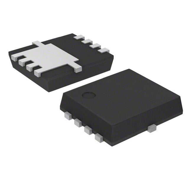
8-VSON-CLIP (5x6)
Package / Case
8-PowerTDFN
CSD19532Q5B Description
## Overview
The Texas Instruments CSD19532Q5B is a high-performance N-channel MOSFET designed for applications requiring low on-resistance, high current handling, and fast switching performance. It belongs to the NexFET™ power MOSFET family, which utilizes advanced trench technology to deliver high efficiency and low gate charge. The device is suitable for synchronous rectification, DC-DC converters, motor drives, and high-efficiency power management applications.
## Electrical Characteristics
The CSD19532Q5B exhibits a combination of low R_DS(on) and low gate charge, optimized for high-frequency switching:
* Drain-Source Voltage (V_DS): 100 V
* Continuous Drain Current (I_D): 77 A at 25°C (with proper thermal management)
* Pulsed Drain Current (I_DM): 310 A
* R_DS(on) Maximum: 1.7 mΩ at V_GS = 4.5 V, 1.5 mΩ at V_GS = 10 V
* Gate-Source Voltage (V_GS): ±20 V
* Total Gate Charge (Q_g): 44 nC typical at V_DS = 80 V, V_GS = 10 V
* Input Capacitance (C_iss): 3,300 pF typical
* Output Capacitance (C_oss): 1,400 pF typical
* Reverse Transfer Capacitance (C_rss): 340 pF typical
The low R_DS(on) ensures minimal conduction losses during high-current operation, while the moderate gate charge allows for efficient switching with minimal driver power requirements.
## Thermal and Power Handling
The CSD19532Q5B is designed for robust thermal performance:
* Maximum Junction Temperature (T_J): 150°C
* Thermal Resistance, Junction-to-Case (R_θJC): 0.56°C/W typical
* Thermal Resistance, Junction-to-Ambient (R_θJA): 62°C/W typical, depending on PCB layout
* Power Dissipation (P_D): 310 W in ideal cooling conditions
Proper heat sinking and PCB copper area are critical to leverage the high current and power capability of this device. The MOSFET’s low R_DS(on) directly reduces thermal stress during high-current conduction.
## Switching Performance
This device is engineered for high-speed switching applications:
* Rise Time (t_r): 17 ns typical
* Fall Time (t_f): 11 ns typical
* Turn-On Delay (t_d(on)): 12 ns typical
* Turn-Off Delay (t_d(off)): 33 ns typical
The combination of low gate charge and fast switching times makes the CSD19532Q5B suitable for synchronous buck converters, high-efficiency motor drives, and other high-frequency power conversion systems.
## Safe Operating Area and Reliability
The CSD19532Q5B features a rugged design:
* Avalanche Energy (E_AS): 150 mJ
* Single-Pulse Avalanche Current (I_AR): 77 A
* ESD Rating: Human Body Model ±2 kV, Machine Model ±250 V
* Latch-Up Immunity: High, owing to NexFET trench design
The robust avalanche capability and ESD tolerance ensure reliable operation in demanding power electronics applications.
## Packaging and Physical Characteristics
* Package: SO-8 or D2PAK-compatible layout (Power-Pak® SO-8)
* Dimensions: Small footprint for high-density PCB designs
* Lead Finish: RoHS-compliant, lead-free solderable finish
* Thermal Pad: Exposed for optimal heat dissipation
The compact package enables designers to implement high-efficiency power stages in limited space while maintaining excellent thermal performance.
## Typical Applications
The CSD19532Q5B is widely used in:
* Synchronous rectifiers in DC-DC converters
* High-frequency switching power supplies
* Low-voltage, high-current point-of-load converters
* Automotive power management circuits
* Brushless DC motor drivers
Its combination of low R_DS(on), high current capability, and fast switching makes it ideal for efficient power conversion in both industrial and automotive environments.
## Summary
The Texas Instruments CSD19532Q5B combines extremely low on-resistance, high current capability, and fast switching performance in a compact Power-Pak® SO-8 package. Its electrical characteristics, thermal robustness, and efficient switching behavior make it suitable for high-efficiency DC-DC conversion, synchronous rectification, and motor drive applications where low losses and high reliability are critical. Proper thermal design and gate drive consideration are key to fully exploiting its performance.
CSD19532Q5B Stock: 28140
5.0 / 5.0

2021-07-09 20:10
Still not auditioned but very fast
2021-08-02 07:24
Felt marking on the packaging not very readable (confusion possible ) ! Without that, conform! Thank you seller!
2021-08-12 12:06
IGBT transistors not detected SA for testerach beside plus t7-h, in tescie for przelaczanie with-12V for E plus zarowka powered + 12V for C triggered finger with Plus, zalancza with-wylancza. Very fast wysylka, fast delivery, product good jakosci, very we
2021-12-31 23:06
Good product and work correctly .
2021-07-09 02:45
Well received, not tested yet